EM47EM3288SBA
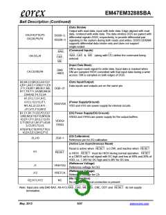
Ball Description (Continued)
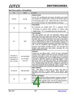
(Data Strobe)
Output with read data, input with write data. Edge aligned with read
data, centered with write data. The data strobes DQS are paired with
differential signals /DQS, respectively, to provide differential pair
signaling to the system during both reads and writes. DDR3 SDRAM
supports differential data strobe only and does not support
single-ended.
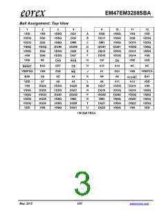
D3,D10,P10,P3
D4,D9,P9,P4
DQS0~3,
/DQS0~3
(Command Inputs)
RAS
,
RAS CAS & WE (along with CS) define the command being
,
entered.
G4,G3,J4
CAS
WE
,
(Input Data Mask)
DM is input mask signal for write data. Input data is masked when
DM are sampled HIGH coincident with that input data during a write
access. DM is sampled on both edges of DQS.
DM0
~MD3
C4,C9,R9,R4
B2,A4,C2,B4,E2,E4,F2,F
4,B11,A9,C11,B9,E11,E9
,F11,F9,M11,M9,N11,N9,
R11,T9,T11,U9,M2,M4,N
2,N4,R2,T4,T2,U4
(Data Input/Output)
Data inputs and outputs are on the same pin.
DQ0~31
A1,G1,L1,U1,A12,
G12,L12,U12,/F1,
M1,A2,J2,U2,A11,
J11,U11,F12,M12
(Power Supply/Ground)
VDD/VSS
VDD and VSS are power supply for internal circuits.
B1,C1,R1,T1,D2,P2,E3,F
3,M3,N3,E10,F10,M10,N
10,D11,P11,B12,C12,R1
2,T12/D1,E1,N1,P1,A3,B
3,C3,R3,T3,U3,
(DQ Power Supply/DQ Ground)
VDDQ and VSSQ are power supply for the output buffers.
VDDQ/
VSSQ
A10,B10,C10,R10,T10,U
10,D12,E12,N12,P12
(ZQ Calibration)
J3,J10
H1
ZQ0~1
RESET
Reference pin for ZQ calibration
(Active Low Asynchronous Reset)
Reset is active when RESET is LOW, and inactive when RESET
is HIGH. RESET must be HIGH during normal operation. RESET
is a CMOS rail to rail signal with DC high and low at 80% and 20% of
VDD, i.e. 1.20V for DC high and 0.30V for DC low.
(Reference Voltage)
Reference voltage for DQ
(Reference Voltage)
Reference voltage for CA
(No Connection)
No internal electrical connection is present.
J1
J12
VREFDQ
VREFCA
NC
G2,H11,H12
Note: Input pins only BA0-BA2, A0-A13,RAS
termination.
CAS
, ,
WE , CS, CKE, ODT and RESET do not supply
May. 2012
5/37
www.eorex.com

 EOREX [ EOREX CORPORATION ]