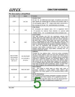
EM47EM1688MBB
4Gb (32M×8Bank
×
16) Double DATA RATE 3 SDRAM
Features
Description
• JEDEC Standard VDD/VDDQ = 1.35V-0.065/+0.1V
• Backward compatible to VDD/ VDDQ = 1.5V ±0.075V..
The EM47EM1688MBB is a high speed Double Date
Rate 3 (DDR3) Synchronous DRAM fabricated with
ultra high performance CMOS process containing 4G
bits which organized as 32Mbits x 8 banks by 16 bits.
This synchronous device achieves high speed
double-data-rate transfer rates of up to 1600
Mb/sec/pin (DDR3-1600) for general applications.
The chip is designed to comply with the following key
DDR3 SDRAM features: (1) posted CAS with
additive latency, (2) write latency = read latency -1,
(3) On Die Termination (4) programmable driver
strength data,(5) seamless BL4 access. All of the
control and address inputs are synchronized with a
pair of externally supplied differential clocks. Inputs
are latched at the cross point of differential clocks
(CK rising and /CK falling). All I/Os are synchronized
with a pair of bidirectional differential data strobes
(DQS and /DQS) in a source synchronous fashion.
The address bus is used to convey row, column and
bank address information in a /RAS and /CAS
multiplexing style. The 4Gb DDR3 devices operates
with a single power supply: 1.35V-0.065/+0.1V & 1.5V
±0.075V VDD and VDDQ. Available package: FBGA-96
Ball (with 0.8mm x 0.8mm ball pitch)
• All inputs and outputs are compatible with SSTL_15
interface.
• Fully differential clock inputs (CK, /CK) operation.
• Eight Banks
• Posted CAS by programmable additive latency
• Bust length: 4 with Burst Chop (BC) and 8.
• CAS Write Latency (CWL): 5,6,7,8
• CAS Latency (CL): 6,7,8,9,10,11
• Write Latency (WL) =Read Latency (RL) -1.
• Bi-directional Differential Data Strobe (DQS).
• Data inputs on DQS centers when write.
• Data outputs on DQS, /DQS edges when read.
• On chip DLL align DQ, DQS and /DQS transition
with CK transition.
• DM mask write data-in at the both rising and falling
edges of the data strobe.
• Sequential & Interleaved Burst type available both
for 8 & 4 with BC.
• Multi Purpose Register (MPR) for pre-defined
pattern read out
• On Die Termination (ODT) options: Synchronous
ODT, Dynamic ODT, and Asynchronous ODT
• Auto Refresh and Self Refresh
• 8,192 Refresh Cycles / 64ms
• RoHS Compliance
• Driver Strength:RZQ/7, RZQ/6 (RZQ=240Ω)
• High Temperature Self-Refresh rate enable
• ZQ calibration for DQ drive and ODT
• RESET pin for initialization and reset function
Oct. 2013
2/38
www.eorex.com

 EOREX [ EOREX CORPORATION ]