EM73P362
4-BIT MICRO-CONTROLLER FOR LCD PRODUCT
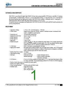
FUNCTION BLOCK DIAGRAM
XOUT
RESET
XIN
P0.0(INT1)/WAKEUP0
P0.1/WAKEUP1
P0.2(INT0)/WAKEUP2
P0.3/WAKEUP3
Sleep Mode
Control
Reset
Control
Clock
Generator
Frequency
doubler
Timing
Generator
W D T
VA
VB
System Control
VEE
LCD
driver
Data pointer
ACC
COM0~COM2
SEG0~SEG14
Stack pointer
Instruction Decoder
Instruction Register
Interrupt
Control
P6,P7,P8/SEG(26..15)
Stack
RAM
ALU
Flag
Low battery detector
Tone generator
BAT
ROM
PC
TONE
Z
C
S
G
HR
12-bit
timer
LR
P4.0(RX)/TONE
P4.1(CS)
Time
Base
(TA)
P4.2(RY)
P4.3(RZ)
I/O Control
High speed counter
PIN DESCRIPTIONS
Pin name
Function
PIN type
VDD
Power supply (+), Power supply (+) for programming OTP
VSS
Power supply (-), Power supply (-) for programming OTP
RESET
System reset input signal, low active
mask option : none
RESET_A
pull-up
XIN
Crystal / external resistor or external clock source
connecting pin
OSC_A / OSC_F
XOUT
P0.0(INT1)/WAKEUP0,
P0.2(INT0)/WAKEUP2
Crystal / external resistor connecting pin
2-bit input pins with external interrupt sources input
and STOP/IDLE releasing function
mask option : wake-up enable, pull-up
wakeup enable, none
OSC_A / OSC_F
INPUT_J
wakeup disable, pull-up
wakeup disable, pull-down
wakeup disable, none
In programming OTP mode:
P0.0/ACLK : address counter clock for programming OTP
P0.2/OEB : data output enable for programming OTP
* This specification are subject to be changed without notice.
11.1.2001
3

 ELAN [ ELAN MICROELECTRONICS CORP ]