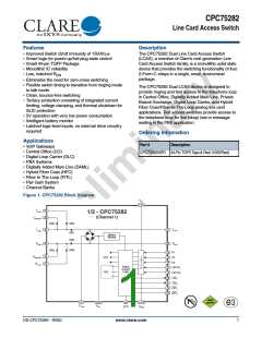
CPC75282
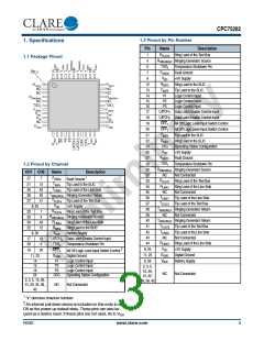
1.3 Pinout by Pin Number
1. Specifications
Pin
Name
RTEST2
RRINGING2
TSD2
Description
Ring Lead of the Test Bus
1
4
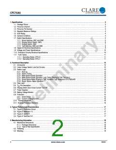
1.1 Package Pinout
Ringing Generator Source
Temperature Shutdown Pin
Fault Ground
6
Pin 1
FGND2
VDD
7
9
+5V Supply
RBAT2
12
Ring Lead to the SLIC
RTEST2
NC
NC
RRINGING2
NC
TSD2
FGND2
VBAT
RTEST1
NC
NC
RRINGING1
NC
TSD1
FGND1
VBAT
TBAT2
13
14
15
16
17
Tip Lead to the SLIC
Logic Control Input
Logic Control Input
Logic Control Input
P1
P2
P3
LATCH1
Data Latch Enable Control Input
Data Latch Enable Control Input
All Off Logic Level Input Switch Control
All Off Logic Level Input Switch Control
Tip Lead to the SLIC
LATCH2
OFF1
VDD
NC
DGND
VDD
CFG
DGND
18
19
OFF2
20
TBAT1
RBAT1
21
22
Ring Lead to the SLIC
Operating States Configuration
+5V Supply
24
CFG
VDD
25
FGND1
TSD1
27
Fault Ground
28
Temperature Shutdown Pin
Ringing Generator Source
Not Connected
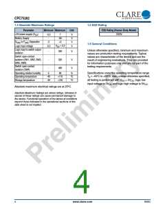
1.2 Pinout by Channel
RRINGING1
30
CH1 CH2
Name
Description
32
NC
1
FGNDx
TBATx
27
21
36
38
37
7
Fault Ground
RTEST1
33
Ring Lead of the Test Bus
Ring Lead of the Line Side
Not Connected
13
42
40
41
Tip Lead to the SLIC
Tip Lead of the Line Side
Ringing Generator Return
Tip Lead of the Test Bus
+5V Supply
RLINE1
34
TLINEx
TRINGINGx
TTESTx
VDD
35
NC
TLINE1
36
Tip Lead of the Line Side
Tip Lead of the Test Bus
Ringing Generator Return
Not Connected
TTEST1
37
9, 25
8, 26
TRINGING1
38
RTESTx
RRINGINGx
RLINEx
RBATx
33
30
34
22
1
4
Ring Lead of the Test Bus
Ringing Generator Source
Ring Lead of the Line Side
Ring Lead to the SLIC
Battery Supply
39
NC
TRINGING2
40
Ringing Generator Return
Tip Lead of the Test Bus
Tip Lead of the Line Side
Not Connected
44
12
TTEST2
TLINE2
41
42
VBAT
43
NC
LATCHx
TSDx
17
28
19
18
6
Data Latch Enable Control Input
Temperature Shutdown Pin
RLINE2
44
Ring Lead of the Line Side
+5V Supply
VDD
DGND
VBAT
2
9, 25
11, 23
8, 26
OFFx
20
All Off Logic Level Input Switch Control
Digital Ground
Digital Ground
DGND
11, 23
14
P1
P2
Logic Control Input
Logic Control Input
Battery Supply
15
2, 3, 5,
10, 29,
31, 32,
16
24
P3
CFG
Logic Control Input
Operating States Configuration
NC
Not Connected
2, 3, 5, 10, 29,
31, 32, 35, 39,
43
35, 39, 43
NC
Not Connected
1
2
“x” denotes channel number
An internal pull-down device is included on this node to set
Off as the power-up default state. These pins can also be
used as a device reset. If these pins are not used, tie to VDD
R00D
www.clare.com
3

 CLARE [ CLARE ]