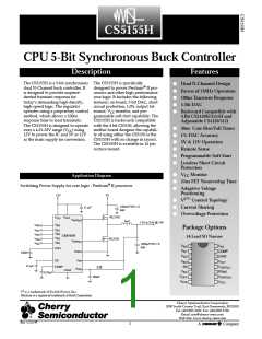
Package Pin Description: continued
PIN SYMBOL FUNCTION
PACKAGE PIN #
16L SO Narrow
7
COFF
VFFB
A capacitor from this pin to ground sets the time duration for the on
board one shot, which is used for the constant off time architecture.
8
Fast feedback connection to the PWM comparator. This pin is connect-
ed to the regulator output. The inner feedback loop terminates on time.
9
VCC2
Boosted power for the high side gate driver.
10
VGATE(H)
High FET driver pin capable of 1.5A peak switching current. Internal
circuit prevents VGATE(H) and VGATE(L) from being in high state simul-
taneously.
11
PGnd
High current ground for the IC. The MOSFET drivers are referenced to
this pin. Input capacitor ground and the source of lower FET should be
tied to this pin.
12
13
14
15
VGATE(L)
VCC1
Low FET driver pin capable of 1.5A peak switching current.
Input power for the IC and low side gate driver.
LGnd
Signal ground for the IC. All control circuits are referenced to this pin.
COMP
Error amplifier compensation pin. A capacitor to ground should be
provided externally to compensate the amplifier.
16
VFB
Error amplifier DC feedback input. This is the master voltage feedback
which sets the output voltage. This pin can be connected directly to the
output or a remote sense trace.
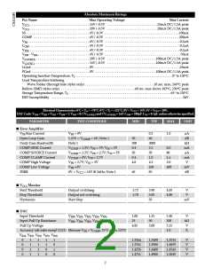
Block Diagram
V
CC2
VCC1 Monitor
Comparator
V
-
CC1
V
GATE(H)
5V
SS Low
Comparator
+
-
FAULT
FAULT
3.90V
3.85V
R
S
Q
Q
+
PGnd
60µA
0.7V
FAULT
Latch
SS
VCC1
SS High
Comparator
+
-
2µA
V
V
ID0
ID1
V
GATE(L)
2.5V
Error
Amplifier
5 BIT
DAC
+
-
V
V
V
ID2
ID3
PGnd
PWM
Comparator
ID4
-
GATE(H) = ON
Q
Q
R
S
Maximum
On-Time
Timeout
+
Slow Feedback
Fast Feedback
V
FB
GATE(H) = OFF
PWM
Latch
C
Normal
Off-Time
Timeout
COMP
OFF
One Shot
R
C
OFF
Extended
Off-Time
Timeout
V
Off-Time
Timeout
FFB
-
S
Q
+
V
Low
FFB
LGnd
Comparator
1V
PWM
COMP
Time Out
Timer
(30µs)
Edge Triggered
5

 CHERRY [ CHERRY SEMICONDUCTOR CORPORATION ]