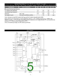
Application Information: continued
When driving large capacitive loads, the COMP must
charge slowly enough to avoid tripping the CS51313 over-
current protection. The following equation can be used to
ensure unconditional startup:
ICHG
I
LIM − ILOAD
<
CCOMP
COUT
where
CHG = COMP Source Current (30µA typical);
COMP = COMP Capacitor value (0.1µF typical);
ILIM = Current Limit Threshold;
LOAD = Load Current during startup;
OUT = Total Output Capacitance.
I
C
Duty Cycle = VOUT / VIN
0.27V / 3.54V = 7% ≈ 5.2%
I
C
Normal Operation
During Normal operation, Switch Off-Time is constant and
set by the COFF capacitor. Switch On-Time is adjusted by
the V2TM Control loop to maintain regulation. This results in
changes in regulator switching frequency, duty cycle, and
output ripple in response to changes in load and line.
Output voltage ripple will be determined by inductor rip-
ple current and the ESR of the output capacitors
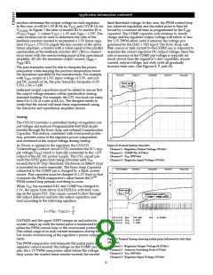
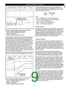
Figure 10: Pulse-by-Pulse Regulation during Soft Start (2µs/div).
Channel 1 - Regulator Output Voltage (0.2V/div)
Channel 2 – Inductor Switching Node (5V/div)
Channel 3 - VCC (10V/div)
Channel 4 - Regulator Input Voltage (5V/div)
If the voltage across the Current Sense resistor generates a
voltage difference between the VFB and VOUT pins that
exceeds the OVC Comparator Offset Voltage (86mV typi-
cal), the Fault latch is set. This causes the COMP pin to be
quickly discharged, turning off GATE(H) and the upper
NFET since the voltage on the COMP pin is now less than
the 1.1V PWM comparator offset. The Fault latch is reset
when the voltage on the COMP decreases below the
Discharge threshold voltage (0.25V typical). The COMP
capacitor will again begin to charge, and when it exceeds
the 1.1V PWM comparator offset, the regulator output will
Soft Start normally (see Figure 11).
Transient Response
The CS51313 V2TM Control Loop’s 200ns reaction time pro-
vides unprecedented transient response to changes in
input voltage or output current. Pulse-by-pulse adjustment
of duty cycle is provided to quickly ramp the inductor cur-
rent to the required level. Since the inductor current cannot
be changed instantaneously, regulation is maintained by
the output capacitor(s) during the time required to slew the
inductor current.
Overall load transient response is further improved
through a feature called “Adaptive Voltage Positioning”.
This technique pre-positions the output voltage to reduce
total output voltage excursions during changes in load.
Because the start-up circuitry depends on the current sense
function, a current sense resistor should always be used.
Holding tolerance to 1% allows the error amplifiers refer-
ence voltage to be targeted +25mV high without compro-
mising DC accuracy. A “Droop Resistor”, implemented
through a PC board trace, connects the Error Amps feed-
back pin (VFB) to the output capacitors and load and carries
the output current. With no load, there is no DC drop
across this resistor, producing an output voltage tracking
the Error amps, including the +25mV offset. When the full
load current is delivered, a 50mV drop is developed across
this resistor. This results in output voltage being offset -
25mV low.
OCP @
VCC > 8.4V
The result of Adaptive Voltage Positioning is that addition-
al margin is provided for a load transient before reaching
the output voltage specification limits. When load current
suddenly increases from its minimum level, the output is
pre-positioned +25mV. Conversely, when load current
suddenly decreases from its maximum level, the output is
pre-positioned -25mV. For best Transient Response, a com-
bination of a number of high frequency and bulk output
capacitors are usually used.
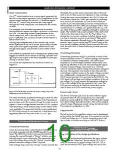
Soft Start @
COMP > 1.1V
Figure 11: Startup with COMP pre-charged to 2V (2ms/div).
Channel 1 - Regulator Output Voltage (1V/div)
Channel 2 - COMP Pin (1V/div)
Channel 3 - VCC (10V/div)
Channel 4 - Regulator Input Voltage (5V/div)
9

 CHERRY [ CHERRY SEMICONDUCTOR CORPORATION ]